Simulation of the PCI-Current Limit Logic of dsPIC33CH

INTRODUCTION
The dsPIC33CH IC has a PCI CL (PWM Control Input-Current Limit) Logic that is use for Current Mode Controlled Converter. An equivalent circuit in LTSPICE is simulated to gain better insights of this logic system. The simulated circuit is based on actual circuit values in the DM330038 dsPIC33CH Curiosity Development Board.
SIMPLIFIED BUCK CONVERTER SCHEMATIC
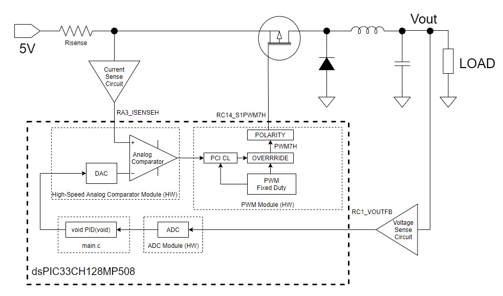
From above figure, we can see that the PCI-CL is part of the PWM Module of the IC.
PCI DIAGRAM
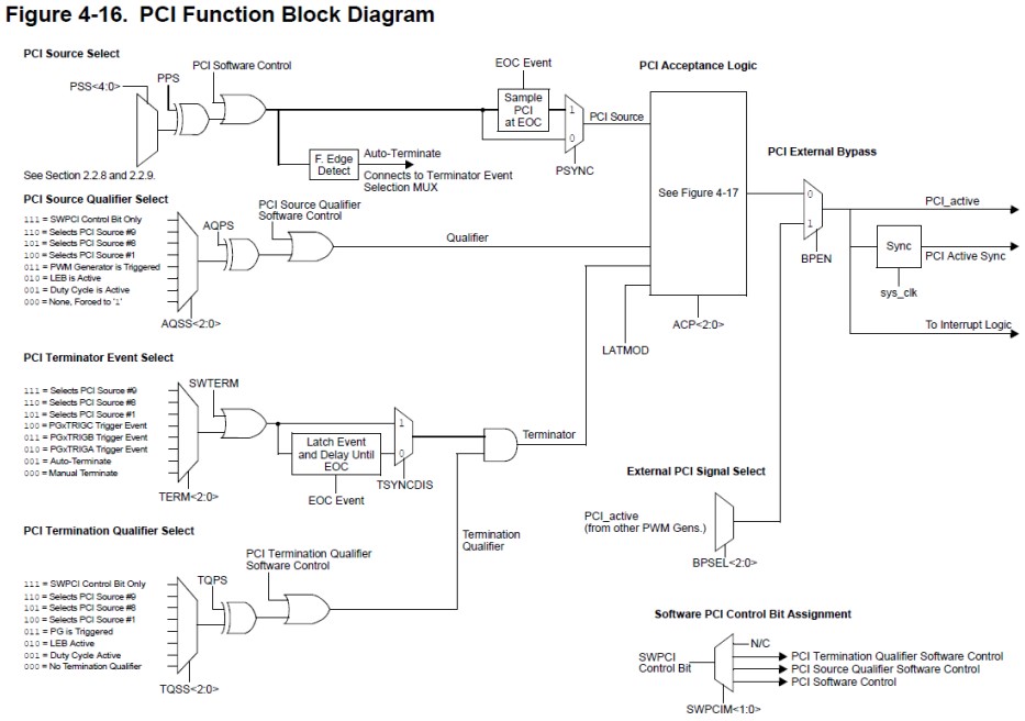
The table below are the register values from above diagram that are needed to configure in order for the PCI to become a current limit logic for the current mode converter:
| Register | Hex Value | Value Definition |
| PSS | 28 | Slave 1 Comparator 1 output |
| PPS | 0 | Not inverted |
| PSYNC | 0 | disabled |
| AQSS | 2 | LEB is Active |
| AQPS | 1 | Inverted |
| TERM | 1 | Auto-Terminate |
| SWTERM | 0 | disabled |
| TSYNCDIS | 0 | PWM EOC |
| TQSS | 0 | No Termination Qualifier, Force 1 |
| TQPS | 0 | Not inverted |
| ACP | 3 | Latched |
| BPEN | 0 | disabled |
| SWPCI | 0 | Drives '0' |
| SWPCIM | 0 | PCI acceptance logic |
By using the values of the registers in the above table. The PCI logic is simplified to the diagram below.
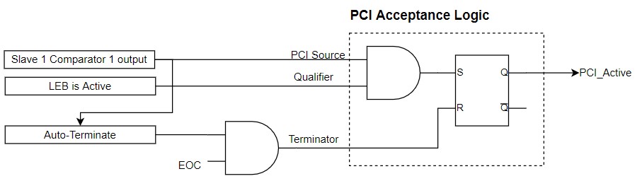
The Leading Edge Blanking (LEB) is a counter circuit that is synchronized with the PWM output and becomes Active after the PWM output becomes high and then resets/stop after the PWM becomes low. The purpose of the LEB is to ignore switching transients.
The Auto-Terminate is a logic circuit that detects falling signal of the comparator output and is reset every start of PWM cycle.
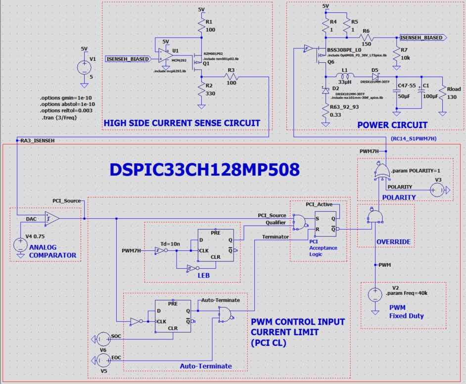
LTSPICE SIMULATION CIRCUIT
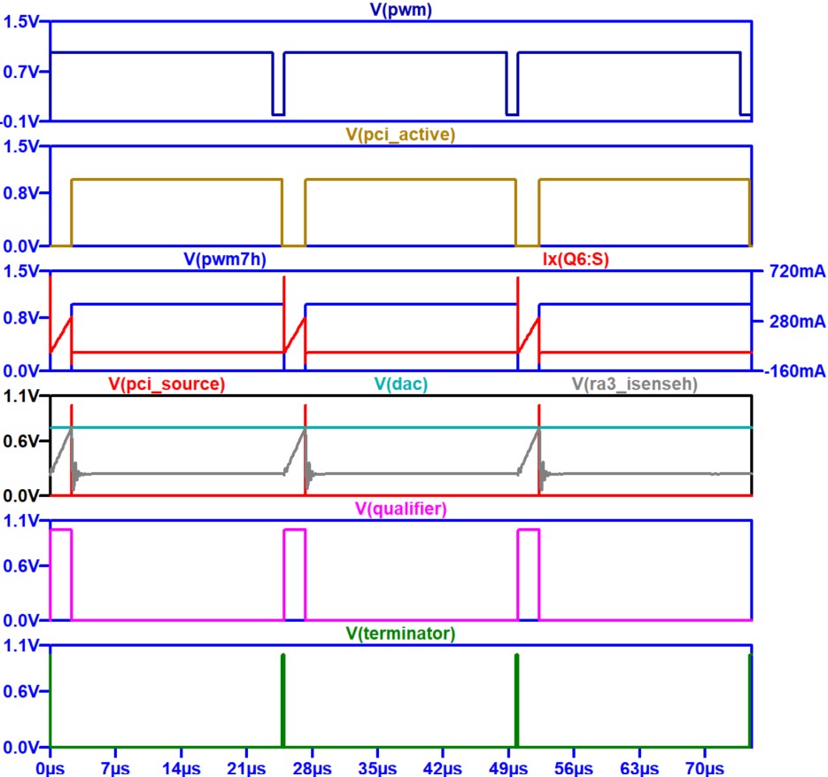
LTSPICE SIMULATION RESULT
LTSPICE Simulation Files: DSPIC33 PCI Current Limit Simulation LTSPICE
Comments