LTspice simulation of hysteretic current control for buck converter

INTRODUCTION
In this article, LTspice simulation of a 5V to 3.3V buck converter using hysteretic current control is presented. The circuit simulated here is the power circuit included in the DM330028 dsPIC33CH Curiosity Developement Board. The control method is an emulation of components and programming of dsPIC33CH. The aim of the simulation is to have an insight on how to configure and program the dsPIC33CH for hysteretic current control.
LTSPICE SCHEMATIC
POWER CIRCUIT
In hysteretic mode, the MOSFET Q6 is switch on until a predetermined peak current is reached. During turn off, the controller will turn on again the MOSFET when the current flowing on the mosfet returns to 0 ampere. The power circuit output level is inherently inversely proportional to the switching frequency of MOSFET Q6 while the duty cycle does not change much. All the components on the power circuit except the Rload resistor can be found on FIGURE A-3 of the DS50002762A document from microchip. I put 100Ω resistor as Rload because it is the one I use as actual load for the 3.3V output. Note also that MOSFET Q6 is a P-Type so a low-level voltage is needed at the gate to turn it on.
HIGH SIDE CURRENT SENSE
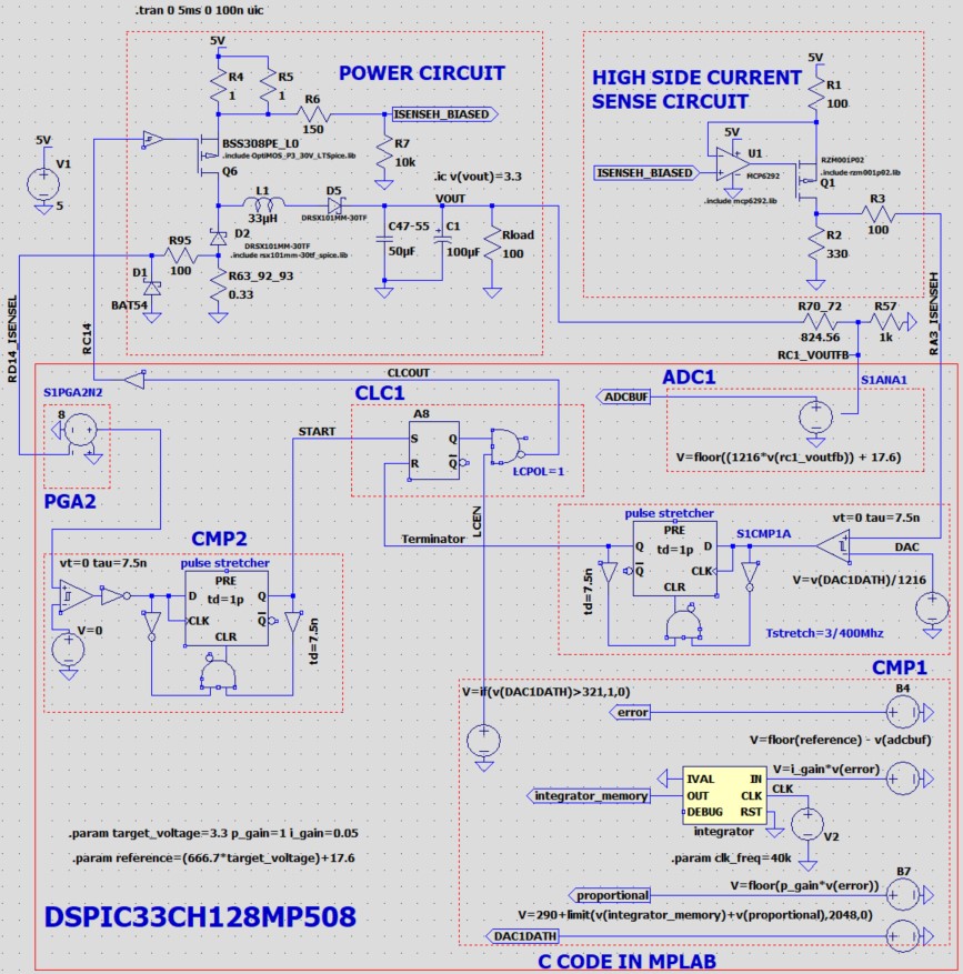
This circuit is used for sensing the current on MOSFET Q6. The output of the high side current sense circuit is fed to the analog comparator CMP1. Below waveform ra3_isenseh is the output of this circuit and compared to the gate drive rc14 waveform. Note that when Q6 is turned off, R63_92_93 is used as low side current sensing circuit instead. All the components on the high side current circuit can also be found on FIGURE A-3 of the DS50002762A document from microchip. The operation of the circuit is also explained in the same document.
ADC1
This ADC module is the one used for sensing the output voltage of the power circuit. The output of the ADC is a digital representation of the sensed output voltage and is fed to or is used by the PID program (C CODE IN MPLAB). This circuit is a mathematical equivalent of the ADC module of the dsPIC33CH. I derived the equation based from my experiment.
CMP1
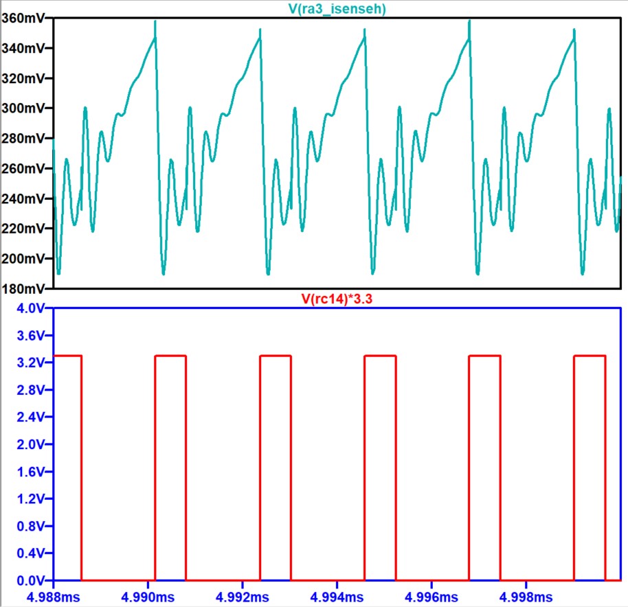
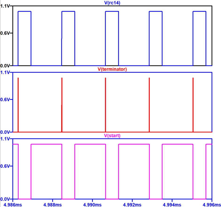
The CMP1 module compares the MOSFET Q6 current (from high side current sense circuit) to the peak current limit PGDC that is calculated by the PID program (C CODE in MPLAB). In MPLAB, i will select 400MHz as the clock frequency of the comparator so I put tau=7.5n (consider also the effect of pulse stretcher). Setting tau=7.5n also will make the simulation faster. The output of the CMP1 is used as terminator for the CLC1 module. Below are the terminator waveform and comparator outputs ra3_isenseh and dac.
C CODE IN MPLAB
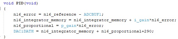
LTspice has no c code so this circuit is just a representation of the PID c code that I will use in MPLAB. Below is the MPLAB PID c code that I usually use. The LTspice element B4 is used to calculate the error which is the difference of the reference and the output of the ADC1. The 2nd line in the PID code below is done by my own LTspice integrator circuit. The integrator circuit operation can be found in this link LTspice integrator. The LTspice element B7 is used to calculate the proportional portion of the PID. The output of the PID is then fed to the DAC1DATH register of ADC1.
PGA2
The low side current sense resistor R63_92_93 of the power circuit has a negative level with respect to the current flow on D2. In order to become positive level, the output of the current sense is fed into the negative input of the PGA (programmable gain amplifier). The PGA gain is set to 8 as recommended in the DS50002762A document. The output of the PGA is fed into another comparator CMP2.
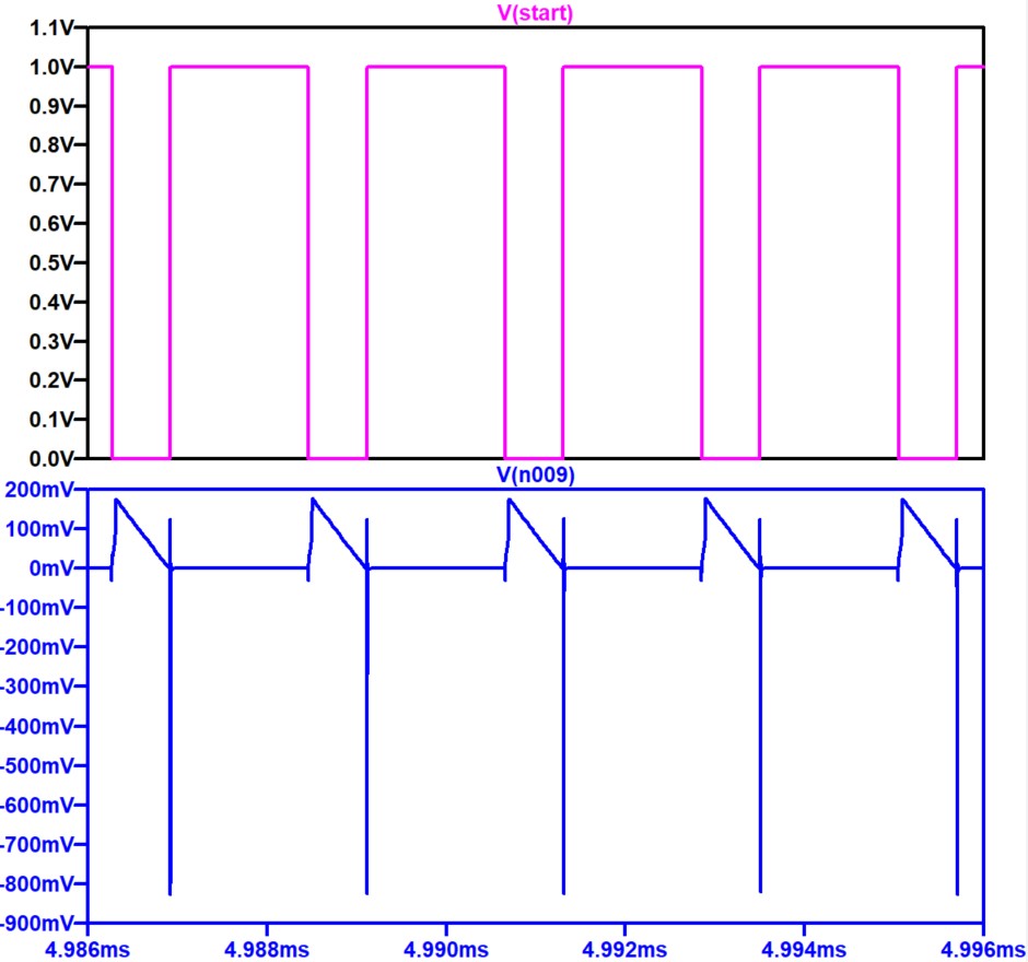
CMP2
This comparator outputs high when the output of the low side current sense becomes 0. The output of this comparator is used to set high the CLC1 circuit. Below is the start waveform and the input to the comparator (blue waveform). The settings of the this comparator is the same with CMP1 except that its negative input is fixed at 0.
CLC1
This circuit is a representation of the dsPIC33's CLC (configurable Logic Cell) configured as an SR flip-flop. This circuit outputs low when START input becomes high and outputs high when Terminator input becomes high.
LTSPICE FILES
Download LTspice files here: LTspice Hysteretic Current Mode Converter
Comments