The dsPIC33CH Curiosity Development Board (DM330028) has a built in buck-boost circuit that we can experiment with. Unfortunately in the time of this writing, the code for the buck-boost converter that is provided by Microchip is only written in assembly language which I found hard to comprehend. So I made my own program that is written in C language and using PID for the close loop control. Only voltage loop control is covered by this topic.
Buck-Boost Converter Circuit
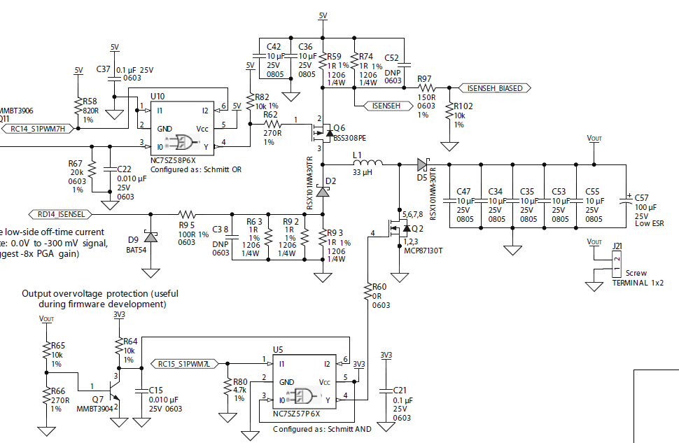
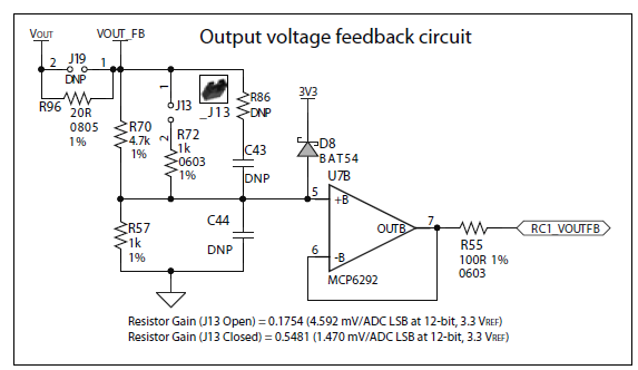
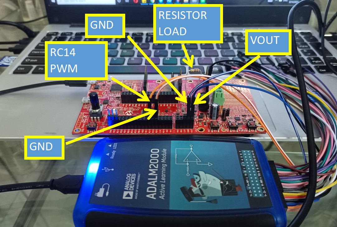
Figure 1 below is the schematic of the buck boost circuit of the DSPIC33CH Curiosity Board. The DSPIC IC can control the buck transistor (Q6) switching through the RC14_S1PWM7H connection. Q6 is a PMOS so it needs a logic 0 (Active-low) to turn it on. The output of the converter (Vout) is sensed by the DSPIC IC through RC1_VOUTFB connection as shown in Figure 2. Make sure that J13 is shorted on the board. Removing the short on J13 will decrease the gain, make the sense voltage small and will have low resolution in the ADC. Removing the short on J13 is useful for boost operation because a higher output voltage will need a lower gain sense resistors. I am connecting a 91Ω resistor as load. For a 3.3V output, the power that will be drawn by the resistor is 3.3V*3.3V/91Ω = 120 milliwatt. RC15_S1PWM7L should be set to low all the time so that the boost transistor (Q2) is always open.
Figure 1 DSPIC33CH Curiosity Board Development Board Buck-Boost Converter Circuit Figure 2 DSPIC33CH Curiosity Development Board Buck-Boost Output Voltage Sense Circuit
CORE SETUP
The PWM control pins in Figure 1 are connected to the Slave Core of the IC so we need to make the source code of the PWM control in the Slave Core. We also need to make a simple source code for the Master Core just to start the Slave Core.
Run MPLAB X IDE (I'm using version v5.50 at the time of this writing). Connect J20 of the Curiosity board to your PC so that the MPLAB application detects what board is connected.
After opening MPLAB, close any projects that are open on the left pane.
MASTER CORE
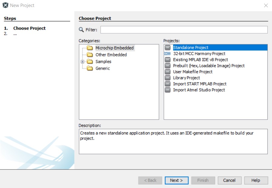
Ctrl+Shift+N to open the new project dialog box. Select Standalone Project then Click Next.
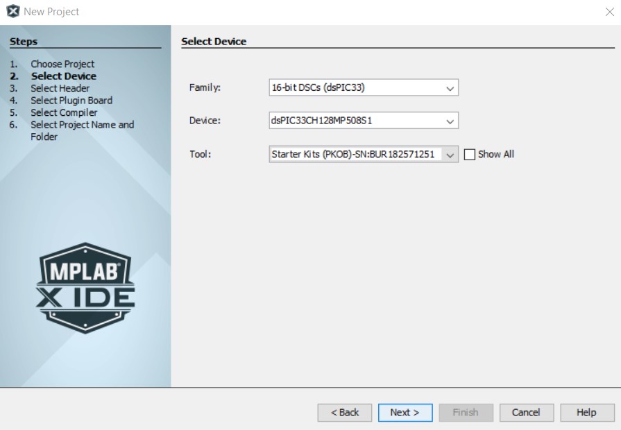
Select Device dsPIC33CH128MP508 and Tool Starter Kits (PKOB)-SN:BUR182571251 then click Next. Note, there is a DM330028-2 version of the Curiosity board so the device and tool will be different. Please refer to its user guide or check the actual part number of the dsPIC IC that is mounted on the board.
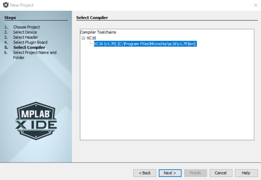
Select Compiler XC16 (v1.70) then click next. You may have a newer version installed.
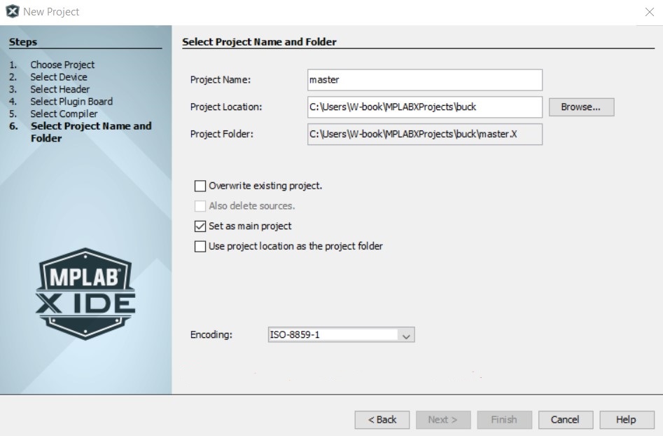
Name the project as "master". I save it to folder "buck" then click Finish.
SLAVE CORE
Ctrl+Shift+N to open again the new project dialog box. Select Standalone Project then click Next.
Again, your Curiosity board may have a different device name but take note of the last two characters ("S1") for the device which means that it is the slave core. Select device dsPIC33CH128MP508S1 and Starter Kits (PKOB)-SN:BUR182571251 then click Next.
Select compiler XC16 (v1.70) then click next.
Name the project as "slave" and use the same project location with the master core. Click Finish.
CODE CONFIGURATION
MASTER CORE
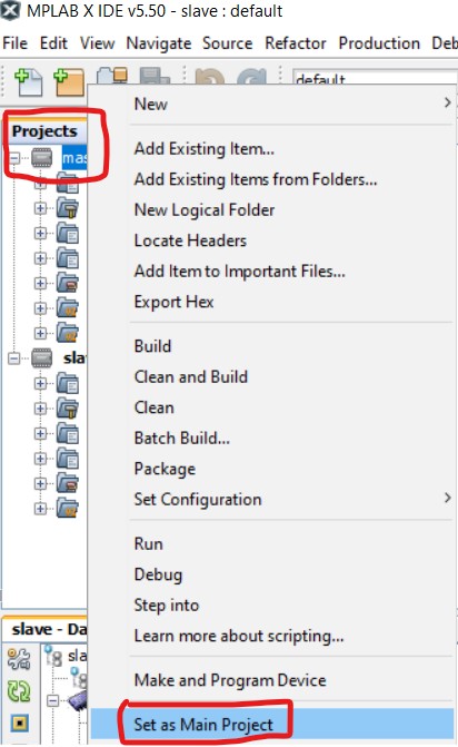
On the Projects Pane, right click on master and select "Set as Main Project".
Click the MCC button on the toolbox. master.mc3 file will be created in the root of the master project folder (..\master.x\master.mc3).
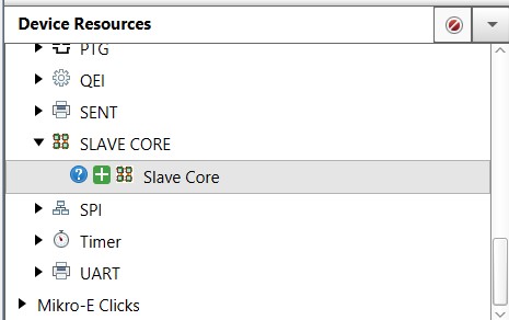
In the device resources pane, click the + on the SLAVE CORE. After clicking it, the SLAVE CORE should appear on the project resources pane.
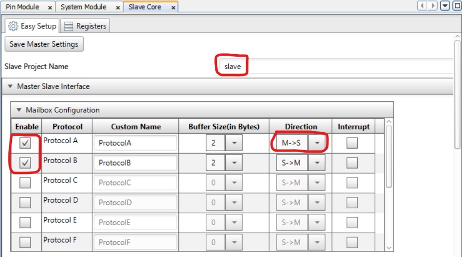
In the Slave Core Pane, name the Slave as "slave". Enable Protocol A and Protocol B. Set Protocol A Direction as M->S.
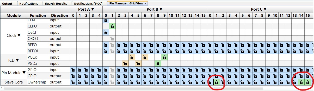
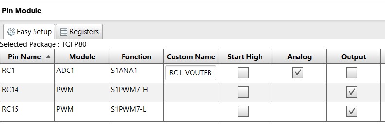
In the Pin Manager Pane, set RC1, RC14 and RC15 as owned by the Slave Core. RC1 is the voltage feedback input. RC14 and RC15 are the PWM pins for controlling the MOSFETs of the buck-boost circuit,
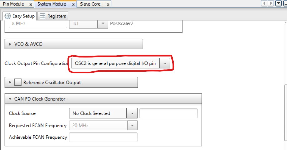
In the System Module Pane, set clock output pin as "OSC2 is general purpose digital I/O pin".
Go back to the Slave Core Pane and click Save Master Settings button. A file named master_config.mc3 will be generated on the root of the master folder after you click the Save Master Settings button.
Lastly for the master configuration, click the Generate button on the Project Resources pane. If there are warnings, review first the Notifications [MCC] pane.
After confirmation on the generate configuration, you should see a Generation complete on the text output. After that, close the configurator by clicking the MCC toolbar button.
SLAVE CORE
On the Projects Pane, right click on the slave project and select Set as Main Project.
Click the MCC button on the toolbox. This will generate a file named slave.mc3 to the root of the slave project folder (..\slave.x\slave.mc3).
Go to the Master Core Pane then click Load Slave Settings from Master Configuration button.
In the Load Master Settings dialog box, browse to the master core folder and open the master_config.mc3 file.
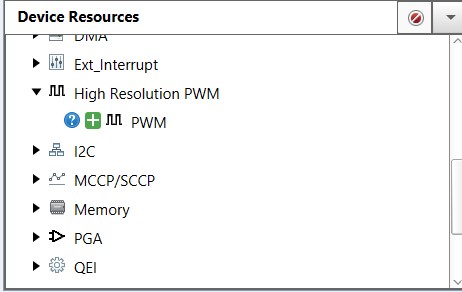
In the Device Resources Pane, click the + on PWM. The PWM will appear on the Project Resources Pane afterwards.
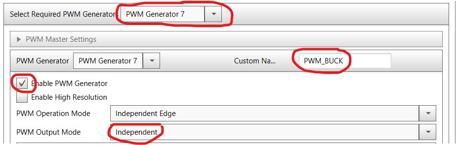
In the PWM Pane, Select PWM Generator 7, rename to PWM_BUCK, enable PWM Generator and change PWM Output Mode to Independent. Note that we can only use Generator 7 because it is the one connected to RC14 and RC15 PWM output.
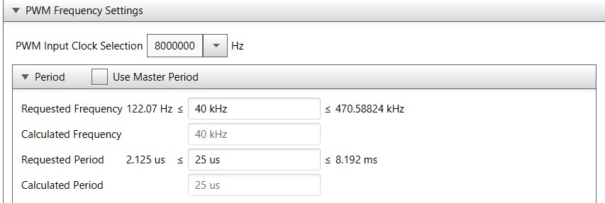
Change the Requested Frequency to 40KHz. Below is the relationship of the Special Function Registers (SFR) to the Independent Edge PWM generator from the dsPIC33/PIC24 FRM High-Resolution PWM with Fine Edge Placement document. Below table defines these SFRs and abbreviations according to my understanding.
Abbreviation
Definition
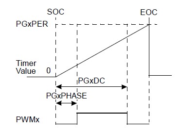
SOC
Start Of Counter
EOC
End Of Counter
PGxPER
PWM Generator x (generator number) Period. The PWM counter counts from 0 up to the value of this SFR. This value is calculated as the value on "PWM Input Clock Selection" (8MHz) divided by the value on "Requested Frequency" (40kHz) less 1 and is equal to 199 (0xC7).
PGxDC
PWM Generator x (generator number) Duty Cycle. The PWM generator output changes to 0 when the counter is equal to the value of this SFR.
PGxPHASE
PWM Generator x (generator number) Phase or deadtime. The output of the PWM generator starts from 0 when counter value is 0 and changes to 1 when the counter value is equal to the value of this SFR.
PWMx
Pulse Width Modulation x (generator number) output. PWMx = 1 if Counter>=PGxPHASE & Counter <= PGxDC else 0. For the dsPIC33 IC that we are using, this output is connected to the RC14 pin.
The initialization of these SFRs will be automatically defined later on a pwm.c file generated by the MCC.
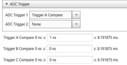
Change the ADC Trigger 1 to Trigger A Compare and Trigger A Compare time to 1ns.
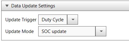
Change the Data Update Trigger to Duty Cycle.
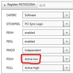
In the Registers tab of the PWM pane, change the POLH to Active-low.
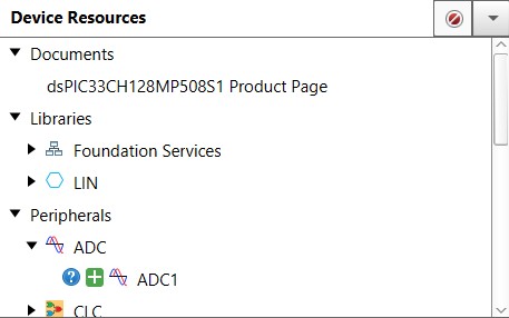
In the Device Resources pane, click + of the ADC1 to transfer the device to the Project Resources.
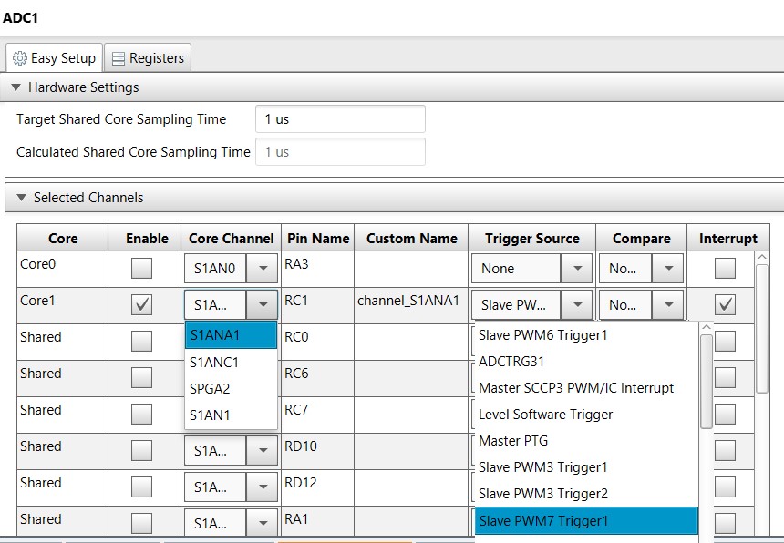
In the ADC1 pane, enable Core1, change Core1 channel to S1ANA1 and Trigger Source to Slave PWM1 Trigger1. Tick the Interrupt Box.
In the Pin Module Pane, change the name of RC1 to RC1_VOUTFB.
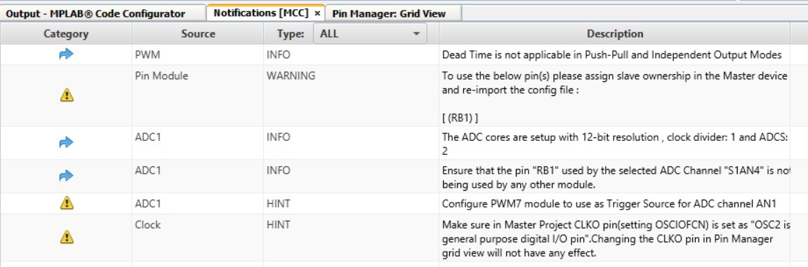
Review the MCC Notifications. Usually I get the warnings like below.
In the Project Resources pane, click Generate button. Click Yes to disregard the warnings and proceed generating the source files. Wait until a "Generation complete" text appears on the MPLAB Code Configurator prompt window.
Close the code configurator by clicking the MCC toolbar button.
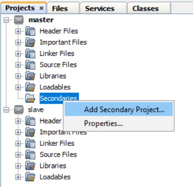
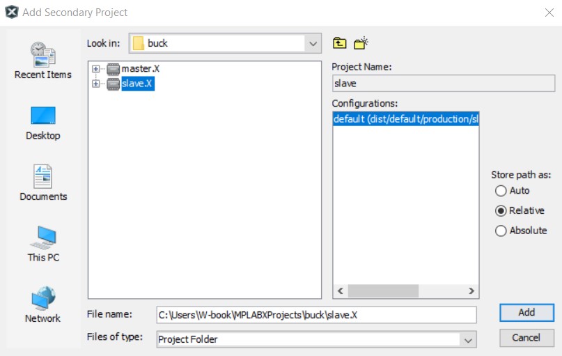
SET THE SLAVE CORE AS SECONDARY PROJECT OF MASTER CORE
Set master project as the main project.
Right click on the Secondaries folder of master project and click Add Secondary Project...
In the Add Secondary Project dialog window, select slave.X and click Add button.
Right-click again on the Secondaries Folder and select Properties. Tick the Build box of the properties dialog window then click OK.
ACTUAL CODING
MASTER CORE SOURCE CODE
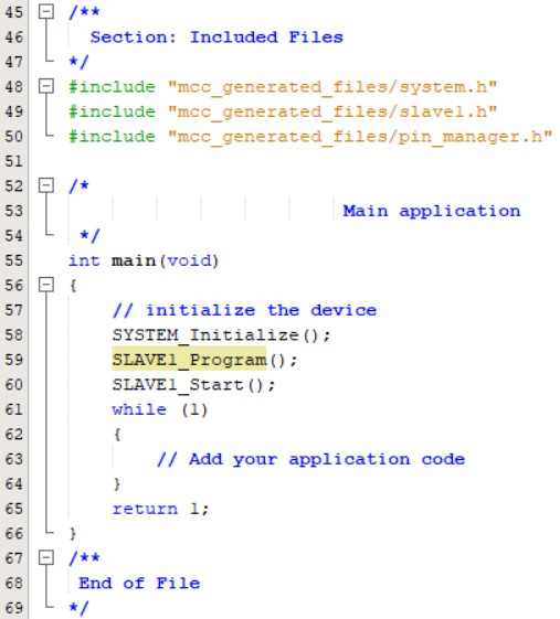
Open the main.c file on the master project's "Source Files" folder.
Below the #include "mcc_generated_files/system.h", add the following codes: #include "mcc_generated_files/slave1.h" #include "mcc_generated_files/pin_manager.h"
Below the SYSTEM_Initialize();, add the following codes: SLAVE1_Program(); SLAVE1_Start();
Below should be how the master core main.c would look like:
Close the main.c file of the master core. Click Save when asked.
SLAVE CORE SOURCE CODE
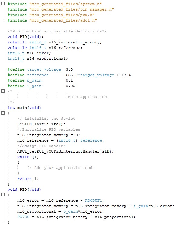
Open the main.c file on the slave project's Source Files folder.
Below the #include "mcc_generated_files/system.h", add the following codes: #include "mcc_generated_files/pin_manager.h" #include "mcc_generated_files/pwm.h" #include "mcc_generated_files/adc1.h"
/*PID function and variable definitions*/ void PID(void); volatile int16_t n16_integrator_memory; volatile int16_t n16_reference; int16_t n16_error; int16_t n16_proportional;
#define target_voltage 3.3 #define reference 666.7*target_voltage + 17.6 #define p_gain 0.1 #define i_gain 0.05 The p_gain and i_gain values are the parameters that you can adjust to fine tune the gain loop response of the buck converter.
Inside the int main(void), add the following codes after SYSTEM_Initialize(); //Initialize PID variables n16_integrator_memory = 0; n16_reference = (int16_t) reference; //Assign PID Handler ADC1_SetRC1_VOUTFBInterruptHandler(PID);
After the int main(void) function, add the following code: void PID(void) { n16_error = n16_reference - ADCBUF1; n16_integrator_memory = n16_integrator_memory + i_gain*n16_error; n16_proportional = p_gain*n16_error; PG7DC = n16_integrator_memory + n16_proportional; }
The new main.c of the slave core should now look like below:
RESULT
Be sure to set the master project as the main project.
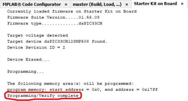
Be sure that the Curiosity board is connected to the PC. Make sure that J13 is shorted on the board.
Click the program button on the toolbar. Wait until the "Programming/Verify complete" is prompted on the Starter Kit on Board Pane.
Below is my hardware setup to validate the result. I use ADALM2000 as oscilloscope.
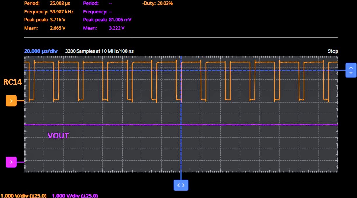
Below is the waveform taken from the ADALM2000 oscilloscope: The mean of the output voltage is 3.22V, a little offset from the 3.3V target. It could be due to the tolerance of the sense resistors, opamp or ADC of the DSPIC IC. The reference in the source code can ba adjusted to compensate this offset. We can also see that the duty measured is 20.03%.


Comments