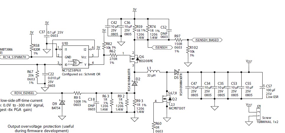
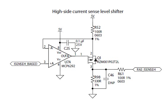
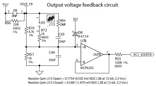
In this article, a hysteretic current control for a 5V to 3.3V buck converter will be implemented in the DM330028 dsPIC33CH Curiosity Development Board. The buck inductor current in a hysteretic current mode flows in a critical conduction so the controller must immediately turn on the MOSFET upon detecting the inductor current has returned to zero. When the MOSFET is turned on, the controller must immediately turn off the MOSFET when the target peak current is reached. The target peak current is calculated by a PID algorithm. Below is the buck/boost circuit of the DM330028 board. There is no direct current sense for the inductor L1 but the high side current sense (R59/R74) resistors can be utilized to measure the rising inductor current when Q6 is on and the low side (R93/R92/R63) current sense resistors can be utilized to measure the decreasing inductor current when Q6 is off. The inputs for the close loop system are the high side current (ISENSEH_BIASED), the low side current (RD14_ISENSEL pin) and the output voltage (Vout). Below is the circuit on the DM330028 board that converts the high side current sense voltage into a level that is within the range of the dsPIC33 input (RA3_ISENSEH pin). The signal on RA3_ISENSEH will be fed to the + input of a built analog comparator of the dsPIC33CH IC. The - input of the comparator is a DAC that will be fed by a calculated value from a PID algorithm. The PID algorithm is based on the sensed voltage from the Vout sense. Below is the output voltage sense circuit. The sensed voltage is RC1_VOUTFB. RC1_VOUTFB will be fed to an ADC and then processed in the PID algorithm.
The third input (RD14_ISENSEL) to the control loop has a negative voltage level when MOSFET Q6 is off and inductor L1 is conducting. This negative level voltage is fed to the -input of a programmable gain amplifier to have a positive output value. The DS50002762A document recommends x8 as the gain setting for this signal. The output of the programmable gain amplifier is then fed to another comparator to detect that the current on the inductor has return to zero.
The first comparator and second comparator outputs are then fed to a built in SR logic circuit as S and R inputs respectively. The output of the SR logic then serves as the drive for MOSFET Q6. For more details or insight on the hysteretic operation, you can check my previous article LTspice - Hysteretic Current Mode Buck Converter.
MASTER CORE GENERATION
The master core here is only used to enable the slave core. All close loop operation will be done on the slave core.
Run MPLAB X IDE (I'm using version v5.50 at the time of this writing). Connect J20 of the DM330028 Curiosity Development Board to your PC so that the MPLAB application detects what board is connected.
After opening MPLAB, close any projects that are open on the left pane.
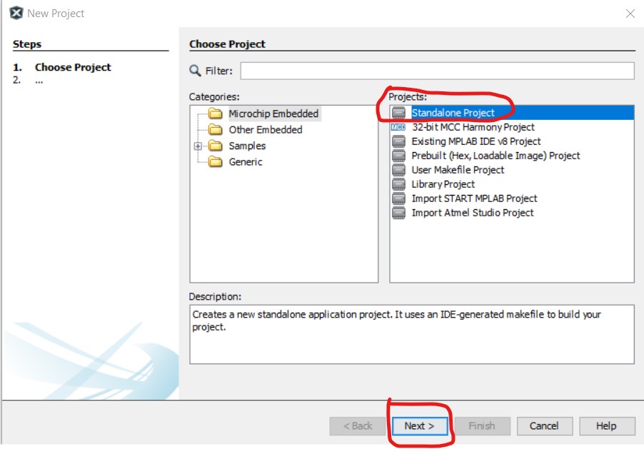
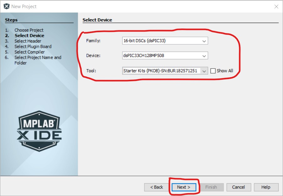
Ctrl+Shift+N to open the new project dialog box. Select Standalone Project then Click Next.
In the Select Device dialog, select "16-bit DSCs (dsPIC33)" as the Family, "dsPIC33CH128MP508" as the Device and "Starter Kits (PKOB)-SN:BUR182571251" as the Tool. Note, there is a DM330028-2 version of the Curiosity board so the device and tool will be different. Please refer to its user guide or check the actual part number of the dsPIC IC that is mounted on the board.
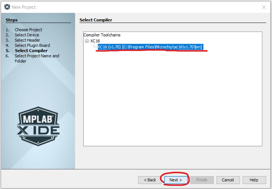
In the next dialog, select Compiler XC16 (v1.70) then click next. You may have a newer version installed.
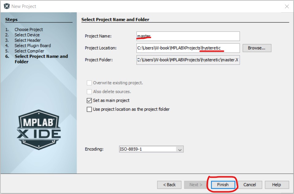
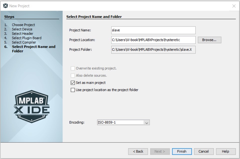
Name the project as "master". I save it to folder "hysteretic". Click Finish.
SLAVE CORE GENERATION
Ctrl+Shift+N to open again the new project dialog box. Select Standalone Project then click Next.
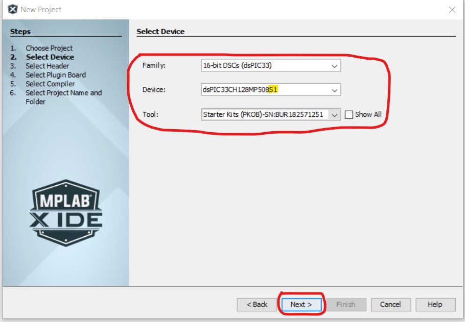
Again, your Curiosity board may have a different device name but take note of the last two characters ("S1") for the device which means that it is the slave core. Select device dsPIC33CH128MP508S1 and Starter Kits (PKOB)-SN:BUR182571251 then click Next.
Select compiler XC16 (v1.70) then click Next.
Name the project as "slave" and use the same project location with the master core. Click Finish.
MASTER CORE CONFIGURATION
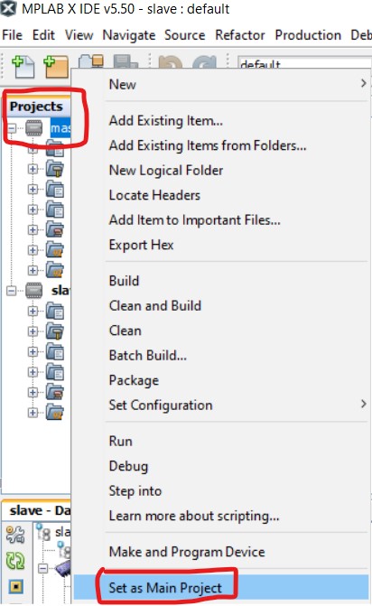
On the Projects Pane, right click on master and select "Set as Main Project".
Click the MCC buttonon the toolbox and wait until the MCC program has loaded. It takes a while to load on my PC. A master.mc3 file will also be discreetly created in the root of the master project folder (..\master.x\master.mc3).
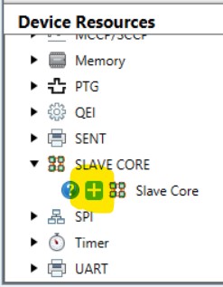
In the device resources pane, click the "+" of the SLAVE CORE. After clicking the "+", the slave core should appear on the project resources pane.
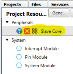
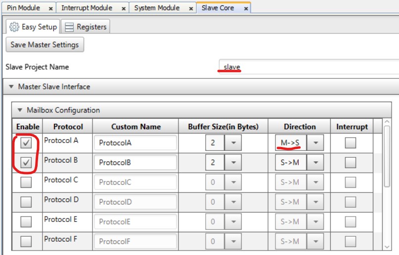
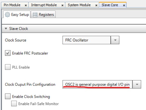
In the Slave Core Pane, name the Slave as "slave". Enable Protocol A and Protocol B. Set Protocol A Direction as M->S. In the Slave Clock settings of the Slave Core pane, set Clock Output Pin Configuration as "OSC2 is general purpose digital I/O pin".
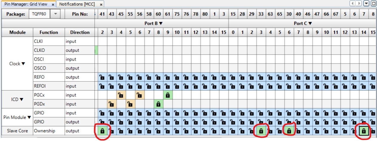
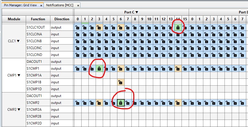
In the Pin Manager Pane, set RB2, RC3, RC6 and RC14 as owned by the Slave Core. RB2 will be used as monitor for an analog signal from DAC inside the dsPIC. RC3 will be used as monitor for the output of the first comparator inside the dsPIC. RC6 will be used as monitor for the output of the second comparator inside the dsPIC. RC14 will be used as the output of the SR logic and used to drive the buck MOSFET Q6.
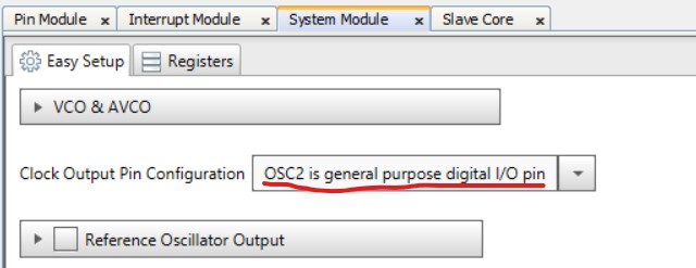
In the System Module Pane, set clock output pin as "OSC2 is general purpose digital I/O pin".
Go back to the Slave Core Pane and click Save Master Settings button. A file named master_config.mc3 will be discreetly generated on the root of the master folder after you click the Save Master Settings button.
Lastly for the master configuration, click the Generate button on the Project Resources pane. If there are warnings, review first the Notifications [MCC] pane.
After confirmation on the generate configuration, you should see a Generation complete on the text output window. After that, close the configuration by clicking the MCC toolbar button.
SLAVE CORE CONFIGURATION
On the Projects Pane, right click on the slave project and select as Main Project.
Click on the MCC button on the toolbar. Wait until the MCC application is completely loaded. A file named slave.mc3 will also be discreetly generated on the root of the slave project folder (..\slave.x\slave.mc3).
Go to the Master Core Pane then click Load Slave Settings from Master Configuration button.
In the Load Master Settings dialog box, browse to the master core folder and open the master_config.mc3 file.
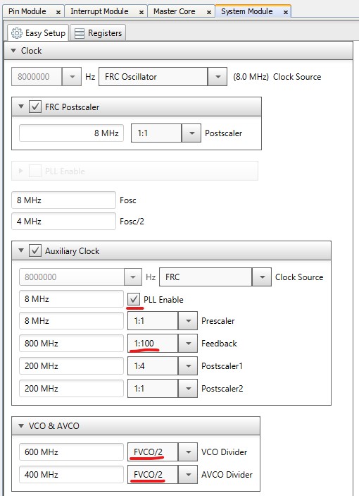
In the System Module tab, tick PLL enable, select 1:100 as Feedback, select FVCO/2 as VCO Divider and select FVCO/2 as AVCO Divider. These settings are needed for the comparator to operate.
In the Device Resources window, click on the "+" of the ADC1 to transfer it to the Project Resources.
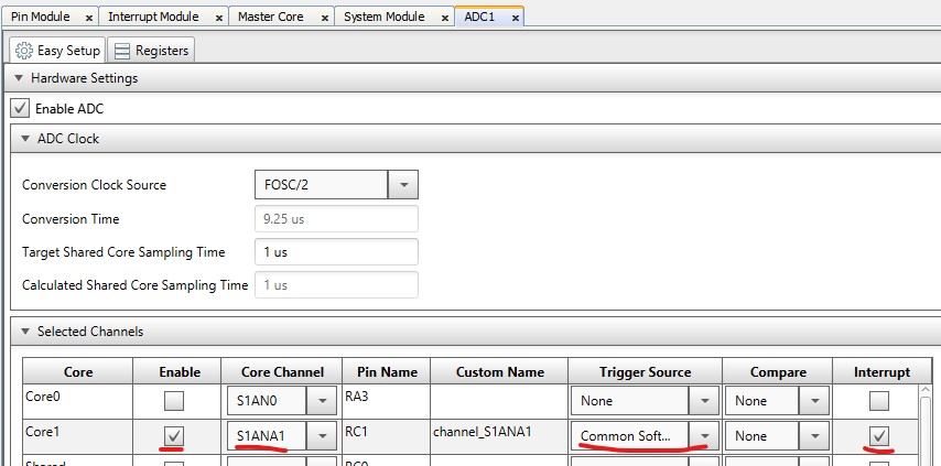
In the ADC1 tab, tick Enable of Core1. Select S1ANA1 as the Core Channel of Core1. S1ANA1 is connected to the RC1_VOUTFB (output voltage sense) of the dsPIC IC. Select Common Software Trigger as the Trigger Source of Core1. Tick Interrupt of Core1.
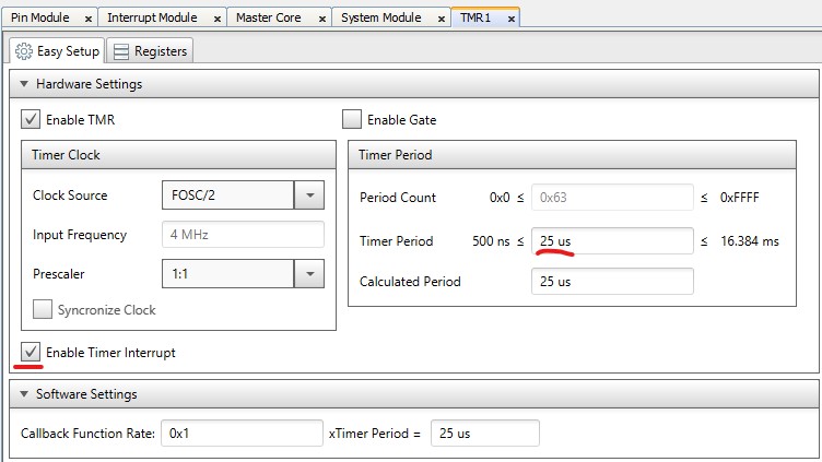
In the Device Resources pane, click the "+" of the TMR1 to move the timer peripheral to the Project Resources.
In the TMR1 tab, type 25 us on the Timer Period and tick the Enable Timer Interrupt. This timer will be used to call the program that will trigger the ADC peripheral that we previously configured.
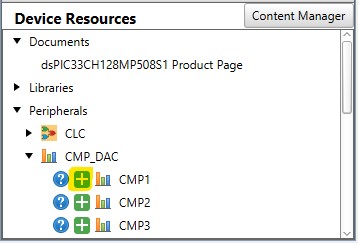
In the Device Resources pane, click the "+" of the CMP1 to move the CMP1 peripheral to the Project Resources.
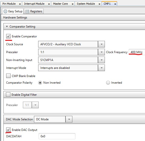
In the CMP1 tab, tick the Enable Comparator, type 400 MHz on the Clock Frequency and tick the Enable DAC output. Note that the Non-Inverting Input default is set to S1CMP1A where RA3_ISENSEH (high side current sense) pin is connected. Ticking the Enable DAC output means that the DAC output that is connected to the inverting input of the comparator will also be connected to DACOUT pin (RB2). We are doing this to monitor the analog output of the DAC.
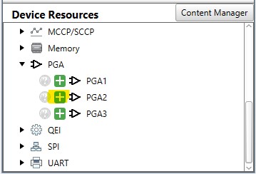
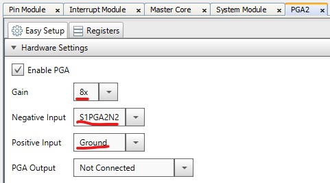
In the Device Resources pane, click on the "+" of the PGA2 (programmable gain amplifier) to move the PGA to the Project Resources. We are selecting PGA2 because it is the peripheral connected to the RD14_ISENSEL (low side current sense) pin of the dsPIC which needs to be amplified with -8 gain.
In the PGA2 tab, change the Gain to 8x, Negative Input to S1PGA2N2 and Positive Input to Ground. S1PGA2N2 is the one that is connected to RD14_ISENSEL pin of the dsPIC. Note that we connect the sense to the negative input and ground to the positive input of the amplifier to have a negative gain.
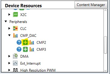
In the Device Resources pane, click on the "+" of the CMP2 to transfer it to the Project Resources.
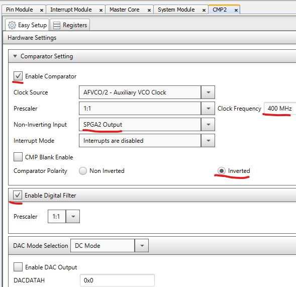
In the CMP2 tab, tick the Enable Comparator, type 400 MHz on the Clock Frequency, select SPGA2 Output as the Non-Inverting Input, tick Inverted and tick Enable Digital Filter.
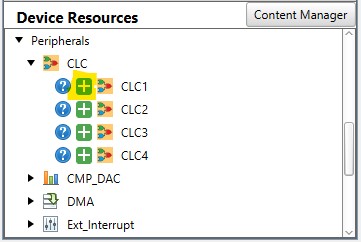
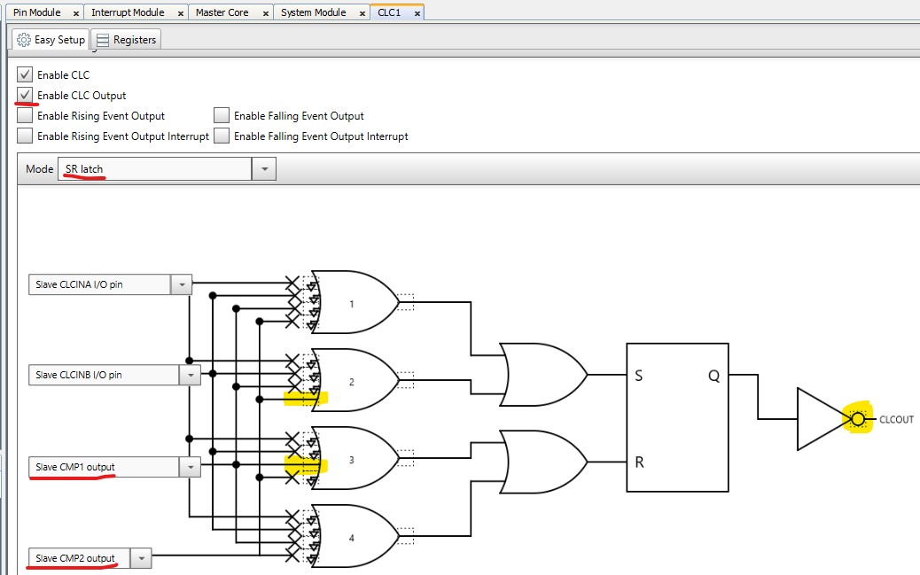
In the Device Resources pane, click the "+" of the CLC1 (Configurable Logic Cell) to transfer it to the Project Resources.
In the CLC1 tab, tick the Enable CLC Output, select SR latch as Mode, select Slave CMP1 output and Slave CMP2 output as inputs of the CLC, Connect Slave CMP1 output to Gate 3, Connect Slave CMP2 to Gate 2 and set the CLCOUT as inverted. The CLCOUT will be configured after to connect to RC14_S1PWM7H pin to drive the buck MOSFET Q6. It is needed to invert the output because Q6 is a p-type MOSFET that need negative gate-source voltage to turn on.
In the Pin Manager Tab, connect S1CLC1OUT to RC14, S1CMP1 to RC3 and S1CMP2 to RC6.
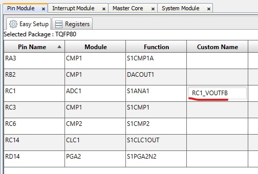
In the Pin Module Tab, type RC1_VOUTFB in the Custom Name of RC1.
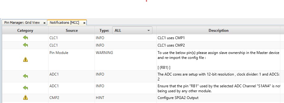
In the Notifications [MCC] tab, review the messages. I usually will have the same as below.
In the Project Resources pane, click Generate button. Click Yes to disregard the warnings and proceed generating the source files. Wait until a "Generation complete" text appears on the MPLAB Code Configurator prompt window.
Close the code configurator by clicking the MCC toolbar button.
ADD SLAVE TO MASTER BUILD
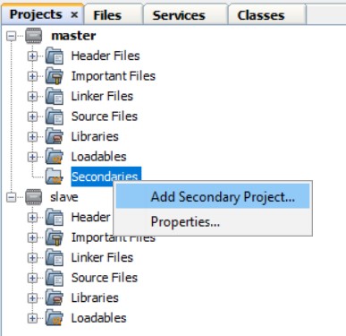
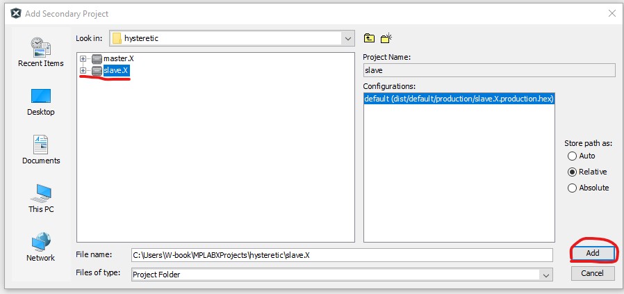
Right click on the Secondaries folder of master project and click Add Secondary Project...
In the Add Secondary Project dialog box, find and select the slave.X folder and click Add.
Right click again on the Secondaries Folder and select Properties. Tick the Build box of the properties dialog windows then click OK.
MAIN PROGRAM
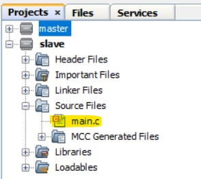
Open the slave project's main.c file.
Replace the main.c file contents with below code. The program has two interrupt handler functions, MyTimer and PID. MyTimer is called every 25us as we configured it on the MCC previously. MyTimer will just enable the software common trigger ( SWCTRG) bit of ADC1. When SWCTRG is enabled, the PID function will be called then the ADC1 will automatically disable back the SWCTRG. The last line of the PID function changes the value of DAC1DATH. DAC1DATH value is the one that is converted into analog that is fed to the CMP1 - input. #include "mcc_generated_files/system.h" #include "mcc_generated_files/pin_manager.h" #include "mcc_generated_files/adc1.h" #include "mcc_generated_files/tmr1.h"
/*PID function and variable definitions*/ void PID(void); void MyTimer(void); volatile int16_t n16_integrator_memory; volatile int16_t n16_reference; int16_t n16_error; int16_t n16_proportional;
Right click on the master project and select Set as Main Project.
Open the master projects main.c file.
Paste the following codes after the line with SYSTEM_Initialize(); SLAVE1_Program(); SLAVE1_Start();
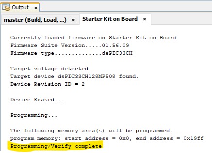
Click the Make and Program Device Main Project button. Wait until Programming/Verify complete is prompted in the text output window.
RESULT
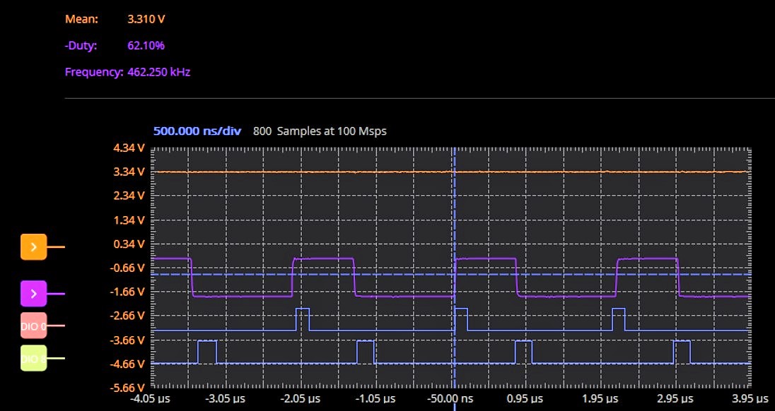
Below waveforms are 3.3V Vout (Orange), Buck MOSFET Q6 drive (Purple) which is measured from pin RC14, CMP1 (Blue 2nd from the bottom) which is measured from pin RC3 and CMP2 (Blue, most bottom) which is measured from pin RC6. Duty is 62% while Frequency is 462kHz. Actually, by ignoring the diode drop and other losses we can confirm the -duty by the formula Vout/Vin = 66% which is near the measured -duty. -Duty is measured here because of the reverse gate voltage requirement of Q6.
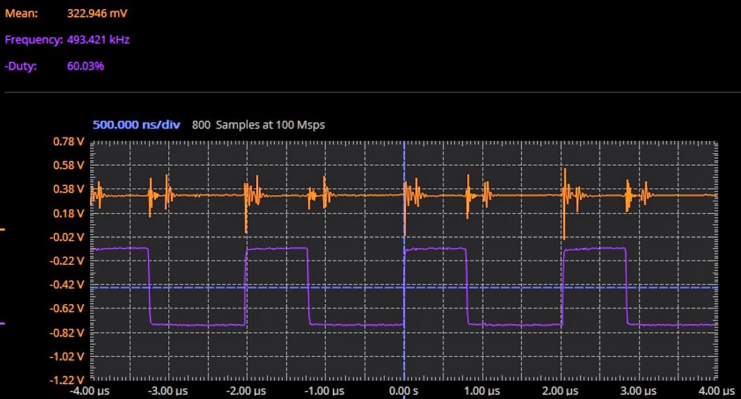
I want to measure the current sense signal on pin RA3 but I realize my scope probe impedance effect is significant for the circuit to handle. When I connect the probe to RA3, the CMP1 output goes abnormal so first I am measuring the voltage on the DAC of CMP1 to know what peak voltage on RA3 before Q6 turns off. Below orange waveform is the DAC waveform and has a mean value of 323mV.
Instead of measuring directly the high side current sense RA3 signal, we can utilize another built-in PGA inside the dsPIC to measure it and then we measure the output of the PGA.
Right click on the slave project and set it as the Main Project.
Click the MCC button on the toolbar menu and wait the MCC application to load completely.
On the Master Core tab, click the Load Slave Settings from Master Configuration button and find/select the master_config.mc3 file.
Add the PGA1 from the Device Resources Pane to the Project Resources.
Click the Generate button on the Project Resources pane then click Yes on the MCC Confirmation warnings dialog box.
Close the MCC application by clicking the MCC button on the toolbar menu.
On the slave project's main.c file, add the following code after the line with TMR1_SetInterruptHandler(MyTimer); . DAC1CONLbits.DACOEN = 0; PGA1CONbits.PGAOEN = 1; These two lines means that the PGA1 is connected to RB2 instead of the CMP1's DAC.
Right click on master project and select Set as Main Project.
Click Make and Program Device Main Project button on the toolbar menu. Wait until Programming/Verify Complete is prompted in the output text window.
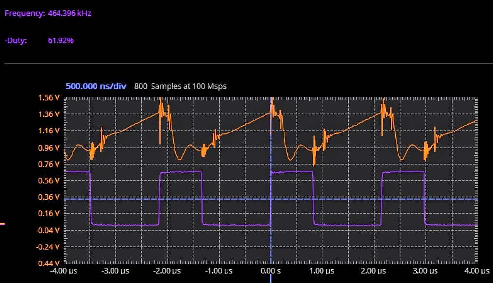
The orange waveform below is the voltage on RB2 which is now the PGA1 output and is the voltage measured on RA3 (high side current sense) multiplied by 4. The peak current is about 1.36V. 1.36V/4 = 340mV which is has similar value with the CMP1 DAC output.
Next we try what waveform we can see on the low side current sense. Since this is also a very small level signal and I do not have a good low impedance probe, we will measure the PGA output instead of measuring directly the signal at pin RD14.
On the slave project's main.c file, change PGA1CONbits.PGAOEN = 1; to PGA2CONbits.PGAOEN = 1;.
Click Make and Program Device Main Project button on the toolbar menu. Wait until Programming/Verify Complete is prompted in the output text window.
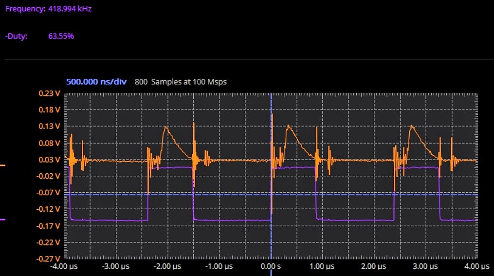
The orange waveform below is now the PGA2 output which is the voltage measured on RD14 (low side current sense) multiplied by 8. I changed the voltage per division to make the signal larger on the screen. The peak voltage is only 130mV. 130mV/8 = 16.25mV is the peak voltage on RD14 which is too small if we use an ordinary passive probe.


Comments