5V to 3.3V Peak Current Mode Buck Converter in the DSPIC33CH Curiosity Development Board

INTRODUCTION
I will demonstrate here how to convert the previous voltage mode buck converter discussed in Voltage Mode Buck Converter to current mode. The code of the voltage mode buck converter is stored here --> Voltage Mode Buck Converter - MPLAB source code.
Before doing the coding, it is good to understand first each circuit and modules.
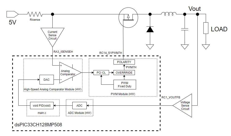
CURRENT SENSE CIRCUIT
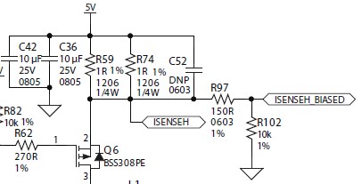
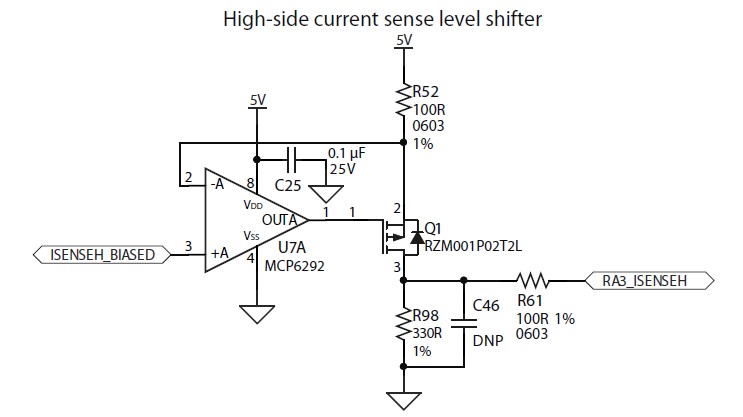
The power MOSFET Q6 high side current sense circuit is shown below. The voltage drop at R59 and R74 resistors is used to monitor the current at Q6. The purpose of R97 and R102 divider resistors is to make a positive bias at the dsPIC analog input pin. According to DS50002762A document, the purpose of the intentional small bias is to ensure that the current sense voltage signal is always within the internal analog comparator input sensing range and the internal DAC reachable range.
I have written the derivation of the equations in mathcad (get mathcad file here) and simulate in LTSPICE (High Side Current Sense LTSPICE Simulation) to easily understand the circuit.
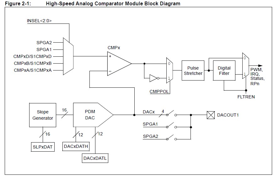
ANALOG COMPARATOR MODULE
PWM CONTROL INPUT CURRENT LIMIT (PCI CL)
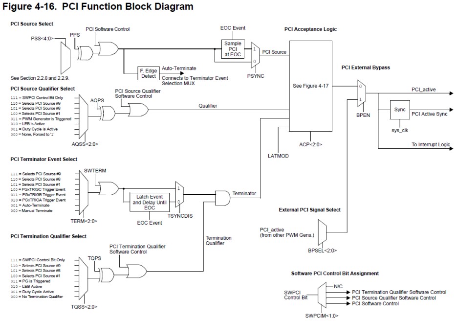
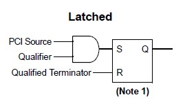
The PCI Acceptance logic block above has three dynamic inputs; PCI Source, Qualifier and Terminator. Its ACP register is set so that it becomes Latched Mode. The Latched Mode logic is shown below.
The input to the PCI Source is set from the analog comparator output. The input to the Qualifier is set as LEB (Leading Edge Blanking Active). The LEB is a counter which starts after PWM7H (PWM output) rises up and resets/stop when PWM7H falls down .The purpose of the LEB qualifier is to prevent unwanted turn off of the PWM during start of cycle due to unwanted transients during switching. The input to the Terminator is the AND of Auto-Terminate and EOC Event. Auto-Terminate becomes high when the analog comparator transitions from high to low. The auto-terminate ensures that the PWM output is turned off while the current is above threshold even if the EOC Event is already reached.
I have simulated the PCI CL with the comparator, PWM and the buck converter circuit in LTSPICE to have better insight about the circuit operation. See PCI Current Limit Simulation.
PROCEDURE
- Save the buck converter files to a different folder.
- Open MPLAB X IDE. After opening, close any opened projects.
- Open the master and slave projects of the voltage mode buck converter.
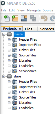
- Ensure that the master project is the main project.
- Click the MCC button and wait the MCC to finish loading.
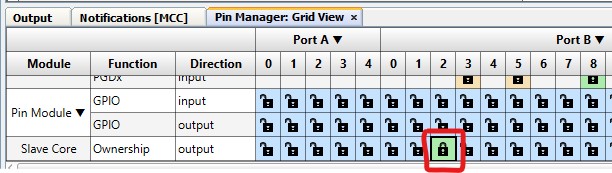
- In the Pin Manager: Grid View, set RB2 as owned by Slave Core. This pin will be used to monitor the the DAC reference for the internal analog comparator by an oscilloscope.
- Click the Slave Core on the Project Resources pane to open the Slave Core Configuration.
- Click Slave Master Settings button.
- In the Project Resources pane, click the Generate button. Wait for the Generation Complete message to appear on the output prompt window.
- Click the MCC button to close the MCC application.
- Go back to the Projects tab on the left pane and set the slave project as Main Project.
- Click the MCC button and wait the MCC to finish loading.
- On the Master Core configuration pane, click the Load Slave Settings from Master Configuration button. Locate and select the master_config.mc3 file that was generated by the master project MCC and then after that click the open button.
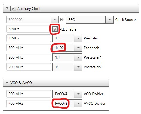
- On the System Module pane, tick PLL Enable, select 1:100 as Feedback and FVCO/2 as AVCO Divider. These frequency settings are needed for the DAC of the Analog Comprator to function properly.
- On the Device Resources pane, click the + of CMP1 to move it to the Project Resources pane.
- On the CMP1 settings, tick Enable Comparator, Enable Digital Filter and Enable DAC Output. The digital filter is utilized to help filter out switching noises. The DAC output does not help on the operation of the comparator but is used to monitor and debug the comparator.
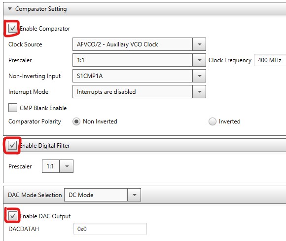
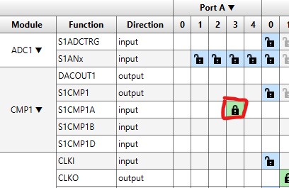
- On the pin manager, let RA3 assigned to S1CMP1A. RA3 pin is connected to the output of the high current sense circuit of DM330038 board. Note that S1CMP1A is the one selected as the non-inverting input of the analog comparator on the above image.
- On the project resources pane, click on PWM to open the PWM configuration.
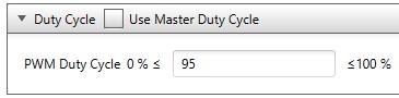
- Set the fixed Duty Cycle to 95%.
- Click on the Registers tab of the PWM settings. Wait the Registers tab to finish loading.
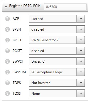
- Change the PG7CLPCIH settings to the same values with the image below. This register contains some of the settings to make the PCI becomes a current limit logic (See PCI-Current Limit Logic for more details).
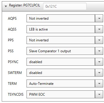
- Change the PG7CLPCIL settings to the same values with the image below. This register contains the other settings to make the PCI becomes a current limit logic (See PCI-Current Limit Logic for more details). Also Slave Comparator 1 output is assigned as the input to the current limit logic.
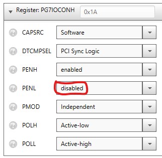
- In the PG7IOCONH register, change the PENL value to disabled. This value ensures that the low side MOSFET does not turn on.
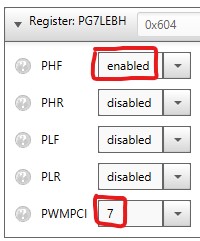
- In the PG7LEBH register, change the PHF to enabled and PWMPCI to 7. The PHF means the PWM7H falling edge will trigger the LEB duration counter. We use a falling edge because we are driving a P MOSFET and a P MOSFET requires a negative polarity drive.
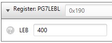
- In Register: PG7LEBL, change the LEB value to 400. This is an arbitrary value and we can change later depending on the result.
- On the Project Resources pane, click the Generate button, click Yes button on the MCC Warning confirmation and wait until Generation Complete message is displayed on the output prompt.
- Click the MCC button to close MCC.
- Open main.c file of the slave project.
- In the PID(void) interrupt handler function, In the last line replace PG7DC by DAC1DATH. Basically, this means that the PID now is now fed to the Slave Comparator 1 negative input instead of directly adjusting the duty cycle of the PWM. At the end of the code append "+260" so that the code now becomes: DAC1DATH = n16_integrator_memory + n16_proportional + 260;. The 260 value is compensation to the offset introduced by current sense circuit.
- On line 62 and 63, Change the p_gain to 0.5 and i_gain to 0.1.
- Set the master project as the Main Project.
- Connect the Curiosity Development Board to the PC.
- Click the make and program device button.
- Wait until the Programming/Verify complete is prompted in the output prompt window.
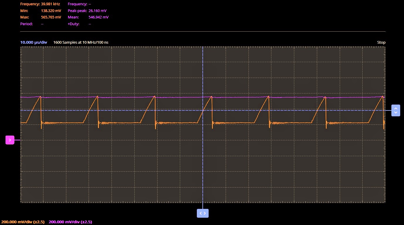
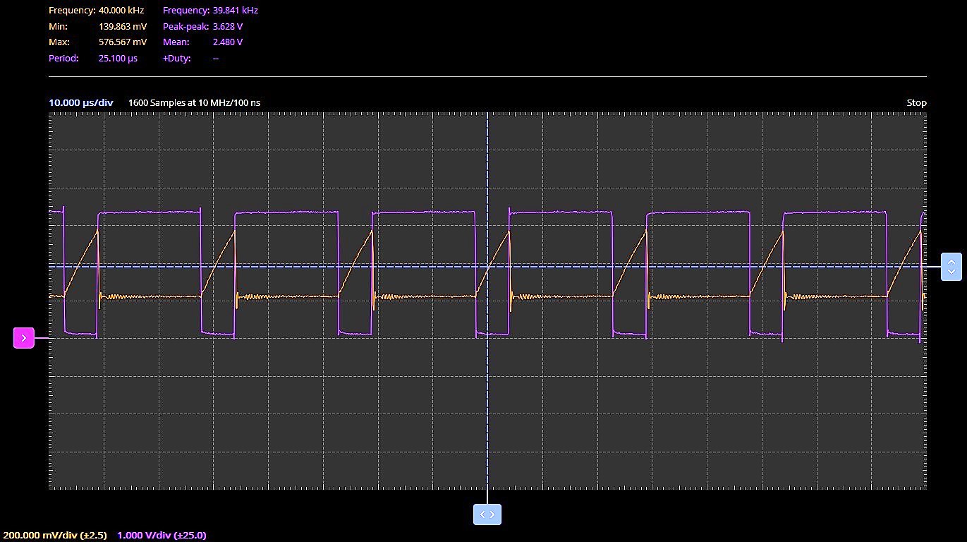
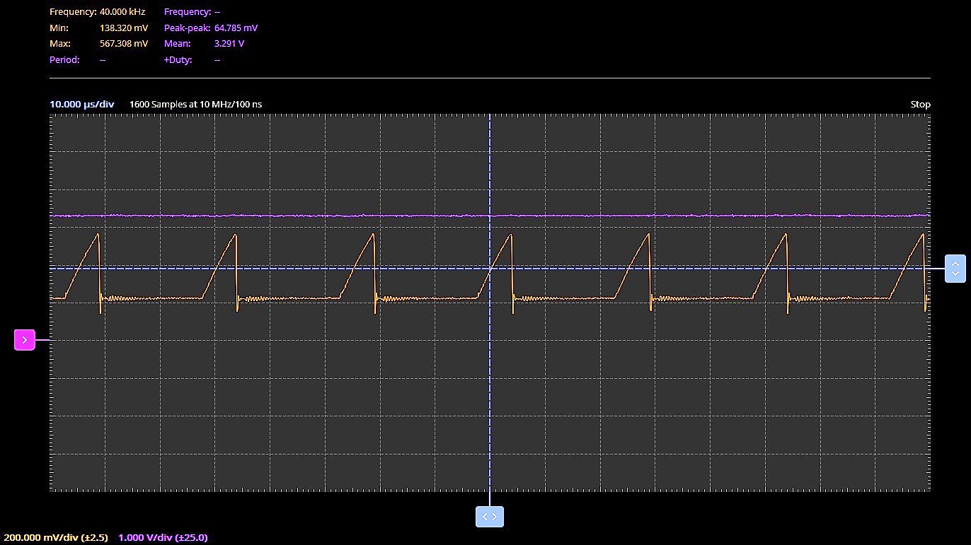
RESULT
Oscilloscope used: ADALM2000
Load:100Ω (Remove power while connecting the load).
Comments